

Union Cabinet approves Rs 4600 crore new semiconductor projects
- In Reports
- 05:58 PM, Aug 12, 2025
- Myind Staff
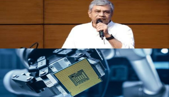
The Prime Minister Narendra Modi-led Union Cabinet on Tuesday approved four new semiconductor projects under the India Semiconductor Mission framework. The semiconductor ecosystem in India had been growing, with six earlier approved projects at different stages of implementation.
The approval of these projects would significantly strengthen the country's semiconductor sector, including the nation's first commercial compound fabrication facility and an advanced glass-based substrate semiconductor packaging unit.
These facilities would support the rising chip design capabilities in the country, backed by government-provided design infrastructure to 278 academic institutions and 72 startups, according to the government statement.
Considering the increasing demand for semiconductors in sectors such as telecom, automotive, data centres, consumer electronics and industrial electronics, these four newly approved semiconductor projects would make a major contribution towards achieving Atmanirbhar Bharat, the release said.
The newly approved proposals came from SiCSem, Continental Device India Private Limited, 3D Glass Solutions Inc., and Advanced System in Package Technologies.
These four newly sanctioned projects would set up semiconductor manufacturing units with a total investment of about Rs 4,600 crore.
The facilities were expected to create jobs for 2,034 skilled professionals and boost the electronic manufacturing sector, which would also lead to additional indirect employment opportunities. With these four new approvals, the total number of India Semiconductor Mission-approved projects rose to 10, with combined investments of about Rs 1.60 lakh crore across six states.
Two major semiconductor facilities SiCSem and 3D Glass, are coming up in Odisha. Continental Device India Private Limited would operate from Punjab, while Advanced System in Package Technologies would be located in Andhra Pradesh.
SiCSem Private Limited, in collaboration with Clas SiC Wafer Fab Ltd. from the UK, was setting up an integrated Silicon Carbide Compound Semiconductors facility in Info Valley, Bhubaneshwar, Odisha.
This commercial compound fabrication unit in India aimed to manufacture Silicon Carbide devices. The facility would have the capacity to produce 60,000 wafers annually and package 96 million units. These components would be used in sectors including missiles, defence equipment, electric vehicles, railways, fast chargers, data centre racks, consumer appliances, and solar power inverters.
3D Glass Solutions Inc. was building an advanced packaging and embedded glass substrate unit in Info Valley, Bhubaneshwar, Odisha. This facility would bring advanced packaging technology to India and improve the efficiency of the semiconductor industry. The unit would use various modern technologies, including glass interposers with passives and silicon bridges, along with 3D Heterogeneous Integration modules.
The planned yearly output included 69,600 glass panel substrates, 50 million assembled units, and 13,200 3D Heterogeneous Integration modules. These products would be important for defence, high-performance computing, artificial intelligence, RF and automotive, photonics and co-packaged optics applications.
Advanced System in Package Technologies would establish a semiconductor manufacturing facility in Andhra Pradesh in collaboration with APACT Co., Ltd from South Korea. The facility would produce 96 million units annually. These products would be used in mobile phones, set-top boxes, automotive parts, and other electronic devices.
Continental Device India Private Limited planned to expand its discrete semiconductor manufacturing unit in Mohali, Punjab. The facility would produce high-power discrete semiconductor components such as MOSFETs, IGBTs, Schottky Bypass Diodes, and transistors, using both silicon and silicon carbide.
This brownfield expansion aimed to reach an annual production of 158.38 million units. These components would be needed for automotive electronics, including electric vehicles and charging infrastructure, renewable energy systems, power conversion applications, industrial purposes, and communication infrastructure.


Comments