


India’s first 3D glass chip packaging unit launched in Odisha
- In Reports
- 01:30 PM, Apr 20, 2026
- Myind Staff
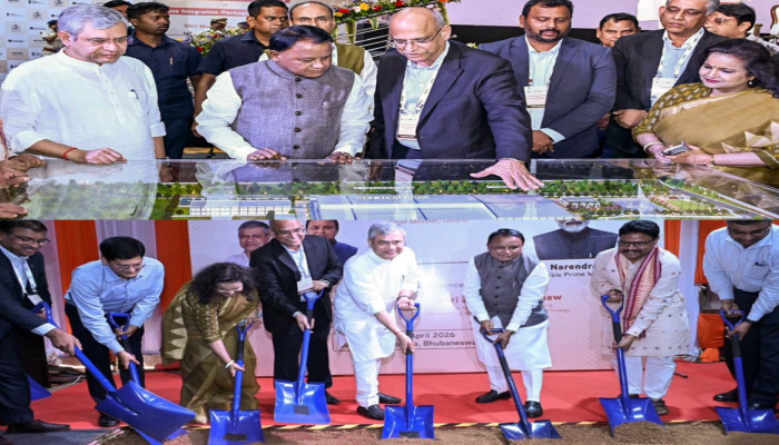
India has taken a major step towards reducing its reliance on imported semiconductor packaging technology with the launch of its first advanced glass substrate-based chip packaging unit in Odisha. On Sunday, Odisha Chief Minister Mohan Majhi laid the foundation stone for this cutting-edge facility in Bhubaneswar. The project marks a significant milestone in strengthening India’s domestic semiconductor ecosystem, especially for critical sectors like artificial intelligence and defence.
The unit is being set up by US-based 3D Glass Solutions Inc. (3DGS) at Info Valley in Bhubaneswar. The project involves an investment of around ₹1,943 crore and will introduce advanced 3D heterogeneous integration (3DHI) packaging technology in India. Until now, the country has largely depended on imports for such high-end semiconductor packaging capabilities. With this development, India aims to bring this advanced technology within its own borders.
Union Electronics and IT Minister Ashwini Vaishnaw attended the groundbreaking ceremony along with Odisha’s IT Minister Mukesh Mahaling. Vaishnaw described the moment as a major achievement for the state and the country. “The state is diversifying from metals and minerals to many new industrial bases,” he said, highlighting Odisha’s growing role as an emerging hub for IT and electronics manufacturing.
He further emphasised the importance of the technology being introduced through this project. “A high-tech industry coming to Odisha is a matter of pride. This is an advanced technology. Normally, a silicone substrate is used in the manufacturing of chips, and now the technology of advanced 3D Glass substrate will be used. The foundation stone of the first major plant using that technology has been laid in Odisha. We will also work to double the capacity of the plant after the completion of the first phase of the plant,” said Vaishnaw.
The facility will operate as a vertically integrated unit, focusing on packaging semiconductor chips for advanced applications. These include artificial intelligence systems, 5G networks, defence technologies, data centres, and high-performance computing. Once fully operational, the plant is expected to produce 69,600 glass panel substrates annually. It will also manufacture around 50 million assembled units and 13,200 3DHI modules each year. In addition to boosting technological capabilities, the project is likely to create more than 2,500 direct and indirect job opportunities.
The core technology used in the unit is based on glass interposers and embedded glass substrates. This marks a shift from traditional organic packaging methods. Glass-based substrates offer better thermal performance and allow for higher integration density. These features are essential for modern, high-performance chips, especially those used in artificial intelligence and data-heavy applications.
This is the second semiconductor-related project to begin construction in Odisha within a short period. Another facility is being developed by SiCSem Private Limited in collaboration with UK-based Clas-SiC Wafer Fab Ltd. This unit, also located at Info Valley, is India’s first commercial silicon carbide (SiC) fabrication plant. It is expected to produce 60,000 wafers and 96 million packaged units annually. The chips produced there will support industries such as electric vehicles, railways, defence, and renewable energy.
Both projects were approved by the Union Cabinet in 2025 as part of a larger national strategy to build a strong semiconductor ecosystem. In total, the government has approved 10 semiconductor projects across the country. These projects together represent an investment of over ₹1.6 lakh crore. The aim is to reduce India’s dependence on imported chips and related technologies, while also positioning the country as a global player in semiconductor manufacturing.
The establishment of the 3DGS unit and the SiCSem facility reflects a broader shift in India’s industrial focus. States like Odisha, traditionally known for their mineral resources, are now moving towards high-tech manufacturing and innovation-driven industries. This transition is expected to create new economic opportunities and strengthen India’s position in global supply chains.
With these developments, India is making steady progress in building a self-reliant semiconductor sector. The introduction of advanced packaging technologies like 3D glass substrates is a key step in that direction. It not only enhances domestic capabilities but also reduces the risks associated with global supply disruptions.
Overall, the new facility in Bhubaneswar represents more than just an industrial project. It signals India’s growing ambition to become a major hub for semiconductor innovation and production. As these projects move forward, they are expected to play a crucial role in shaping the future of technology manufacturing in the country.


Comments