


India approves 23 chip design projects under ₹76,000 crore Semicon India program
- In Reports
- 07:16 PM, Jul 31, 2025
- Myind Staff
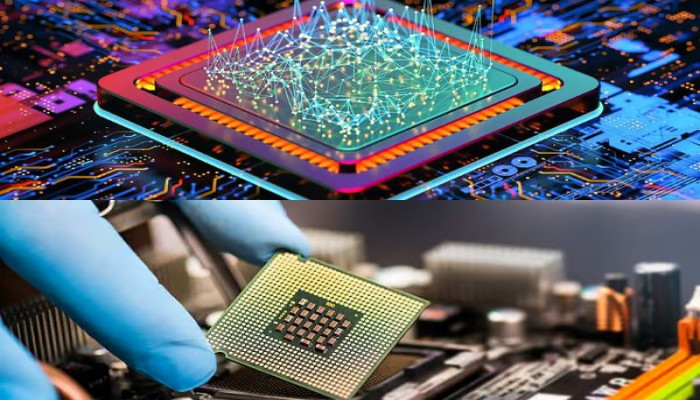
In a move to strengthen India's semiconductor design and manufacturing capabilities, the central government has cleared 23 chip design projects under the Design Linked Incentive (DLI) scheme. The announcement was made in the Lok Sabha by Union Minister of Electronics and Information Technology, Jitin Prasada.
As reported by DD News, the approved projects, mainly led by Indian start-ups, MSMEs, and domestic firms, will receive government support to develop chip solutions for a range of applications, including surveillance cameras, energy meters, microprocessor IPs, and networking systems.
The Design Linked Incentive scheme forms a part of the broader ₹76,000 crore Semicon India Program, which was launched to build a full-scale semiconductor and display manufacturing ecosystem in the country.
Since its inception in December 2021, the initiative has seen participation from around 278 academic institutions and 72 start-ups, who have gained access to advanced Electronic Design Automation (EDA) tools, according to DD News.
To steer this mission, the government established the India Semiconductor Mission as a dedicated unit under the Digital India Corporation. The Mission has been granted financial and administrative autonomy to implement India’s long-term plans in semiconductor design, fabrication, and display manufacturing.
Under the Semicon India Programme, four major schemes were rolled out.
The first scheme supports the establishment of Semiconductor Fabs in India, encouraging large investments for chip wafer fabrication units. The financial support varies by chip node size—up to 50 percent of the project cost for technologies using 28nm or smaller nodes, up to 40 percent for 28nm to 45nm nodes, and up to 30 percent for nodes between 45nm to 65nm.
The second scheme supports the creation of Display Fabs, offering up to 50 percent of the project cost, with a maximum cap of ₹12,000 crore per unit. This scheme targets technologies such as TFT LCD and AMOLED.
The third initiative provides support for Compound Semiconductors, Silicon Photonics, Sensors Fab, and OSAT (Semiconductor Assembly, Testing, Marking, and Packaging) facilities. It covers 30 percent of capital expenditure for companies planning to set up such facilities in India.
The fourth, the Design Linked Incentive scheme, offers financial and infrastructural support across the chip design process. It includes a Product Design Linked Incentive of up to 50 percent of eligible costs, capped at ₹15 crore per application, and a Deployment Linked Incentive ranging from 6 percent to 4 percent of net sales turnover for five years, with a maximum cap of ₹30 crore per applicant.
In addition to these schemes, the government has approved the upgradation of the Semi-Conductor Laboratory in Mohali, aiming to convert it into a brownfield fabrication unit.


Comments