


India achieves major breakthrough in GaN semiconductor technology, joins elite global group
- In Reports
- 04:28 PM, Jan 27, 2026
- Myind Staff
In 2023, Indian military scientists achieved a major technological breakthrough that quietly placed India among a small group of advanced nations in the field of compound semiconductors. Working in close coordination between Delhi and Hyderabad, researchers successfully developed gallium nitride monolithic microwave integrated circuits (GaN MMICs), a highly advanced semiconductor technology used in modern defence systems. With this achievement, India reduced its dependence on foreign countries for some of the most critical and high-value semiconductor components.
This milestone positioned India alongside countries such as the United States, France, Russia, Germany, South Korea and China. The development marked an important step in India’s journey toward technological self-reliance and strengthened its strategic capabilities in defence and advanced electronics.
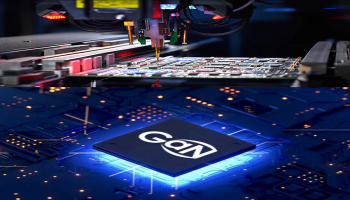
The breakthrough took place inside the Solid State Physics Laboratory (SSPL), one of the most sensitive research facilities under the Defence Research and Development Organisation (DRDO). The laboratory has a state-of-the-art clean room spread across 1,300 square metres. This environment is carefully controlled to prevent even microscopic contamination during the semiconductor fabrication process.
Inside the clean room, scientists wearing sterilised overalls and caps celebrated the success of years of effort. Advanced machines stood silently around them as their long journey of research and development reached a decisive moment. The scene reflected both the intensity of scientific work and the importance of the achievement for national security and technological independence.
MMICs, also known as compound semiconductors, are made from materials that combine more than one element. Unlike traditional silicon chips, compound semiconductors offer higher performance, greater efficiency and faster switching speeds. They can also operate reliably in extreme conditions, which makes them essential for advanced military applications.
These chips are valued for their chemical stability and ability to withstand very high temperatures and voltages, along with low transmission loss. Because of these properties, they are ideal for defence systems where performance and reliability are critical.
Along with GaN, gallium arsenide (GaAs) compound semiconductors are also widely used. Both GaN and GaAs outperform silicon in high-frequency data transmission, but they serve different purposes based on power requirements. GaAs chips are suitable for low to moderate power applications and microwave systems, making them useful in mobile phones, satellites and communication technologies.
GaN chips, however, are designed for much more demanding environments. They have superior electron mobility and are built to handle high power and high temperatures. These chips can function at temperatures of up to 1,000 degrees Celsius, making them indispensable for advanced military hardware.
Despite their small size, GaN chips are extremely powerful. A single GaN chip capable of delivering 30 watts measures only 3.5 mm by 3 mm, yet it can switch power nearly 300 times faster than a silicon-based chip. This unique combination of size, speed and power explains why GaN MMICs are widely used in advanced military drones, missile systems, radars, fighter aircraft and naval platforms.
Compound semiconductors also play a crucial role in sensors. These sensors detect movement, heat, sound, light and pressure, converting physical changes into electronic signals. These signals are used to guide weapons and monitor the performance of complex defence systems in real time.
India’s journey into compound semiconductor technology began decades ago. In the 1990s, Indian scientists successfully developed GaAs semiconductor technology, which was considered a major achievement. However, GaN MMICs remained beyond reach for many years due to their complexity and the extreme precision required in their fabrication.
The long-standing challenge was finally overcome in 2023, when Indian researchers made a GaN breakthrough that had eluded them for so long. With sustained effort, technical expertise and continuous innovation, scientists achieved this rare feat.
Meena Mishra, Director of SSPL, described the breakthrough as a moment of shared joy for the entire SSPL and GAETEC team. Reflecting on her 35 years at the laboratory, she highlighted the long and demanding nature of the technology development process. She explained that each fabrication and testing cycle takes around 80 days and involves hundreds of highly precise steps, all of which must be executed perfectly.
Only after careful optimisation of every stage is a final production run attempted. Using a simple metaphor, she said, “The dough is now ready, and India can choose to make any kind of bread it wants from it.” Her words captured both the technical achievement and the vast potential of the technology that India now possesses.
The successful development of GaN MMICs represents more than a scientific accomplishment. It is a strategic milestone that strengthens India’s defence preparedness and reduces vulnerability to global supply chain disruptions and geopolitical pressures. With this capability now firmly established, India has created a strong foundation for next-generation radars, missiles and electronic warfare systems built entirely on indigenous technology.
This breakthrough reflects decades of scientific effort and marks a decisive step in India’s pursuit of technological independence. By mastering GaN semiconductor technology, India has entered an exclusive global club and opened new possibilities for advanced defence systems and high-performance electronics, all developed within the country.


Comments