




IISc, Samsung launch Quantum Lab to boost India’s next-gen tech research
- In Reports
- 06:45 PM, Oct 15, 2026
- Myind Staff
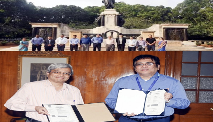
The Indian Institute of Science (IISc) and Samsung Semiconductor India Research (SSIR) inaugurated a Quantum Research Lab at IISc on Thursday to strengthen India’s research capabilities in quantum technologies and advanced semiconductors.
Supported by Samsung’s corporate social responsibility (CSR) funding, the lab will focus on quantum devices, cryogenic electronics, which operate at extremely low temperatures, and advanced materials for future technologies.
Quantum technologies use the unusual behaviour of matter at atomic and subatomic scales. Unlike conventional computers, which process information using bits representing zero or one, quantum computers use quantum bits (qubits) that harness quantum effects to perform certain calculations differently. Developing reliable qubits and systems to control them remains a major challenge.
The facility will focus on qubit characterisation, cryogenic electronics, quantum-device reliability, and single-photon sources and detectors. Single photons are individual particles of light that can carry quantum information, making them important for quantum communication and other applications.
Researchers will also study two-dimensional (2D) materials, which are extremely thin and may have different properties from their bulk counterparts. The research will include developing and studying 2D-material-based quantum devices under cryogenic conditions.
The collaboration aims to make specialised research infrastructure accessible to students and researchers beyond IISc. High equipment costs and operational expenses often limit access to such facilities. The lab will address this gap through structured training and research opportunities.
The partnership will also link quantum research with semiconductor skills development through the India Semiconductor Workforce Development Program (ISWDP). The programme addresses skill gaps in device physics, process development, modelling, simulation, characterisation and reliability. Selected modules will cover quantum materials and devices, cryogenic electronics and qubit technologies.
Prof Mayank Shrivastava, chair of IISc’s Department of Electronic Systems Engineering and lead for both initiatives, said the aim was to build capabilities across semiconductor education and advanced research. He said the workforce programme was giving thousands of learners practical exposure to semiconductor workflows, while the new lab was advancing research into 2D-material-based quantum devices, including qubits and single-photon detectors.
Samsung Semiconductor India Research managing director Rajesh Krishnan said semiconductors and quantum were poised to be the next wave of innovation, making talent critical to India’s technology ambitions, and industry-academia collaboration could create lasting impact through infrastructure, education and access.
IISc director Prof Govindan Rangarajan said Samsung’s support had enabled IISc to strengthen frontier quantum research and semiconductor workforce development, complementing its larger role in advancing national capabilities in quantum computing and next-generation semiconductor technologies.
The initiative comes as India seeks to expand domestic expertise in semiconductors and quantum technologies.



 Loading...please wait
Comments